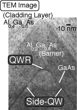
TEM image

Very thin GaAs actuve layer is slowly curved at the top of the ridge structure.
The vertical thickness of GaAs active layer in QWR is thicker than in side-QW, so carriers are well confined in this crescent shaped QWR region.
The size of our QWR structure is 5 nm of vertical thickness and about 20 nm of lateral confinement width.
Carriers confined in this QWR region can only move along this one dimensional perpendicular direction.
The structure is further sandwiched between another AlGaAs cladding layer, and formed an optical waveguide structure.
((Back to the former page))
The sample is cleaved in 300 mm to form optical cavity structures.
Next Page